Project information
- Course: ECE 4740 — Intro to Digital VLSI
- Date: April 7 – April 21, 2025
- Tools: Cadence Virtuoso (Schematic & Layout), SPICE, DRC, LVS, Monte Carlo Simulation
600ps
Cycle time
14.2fJ
Read energy/bit
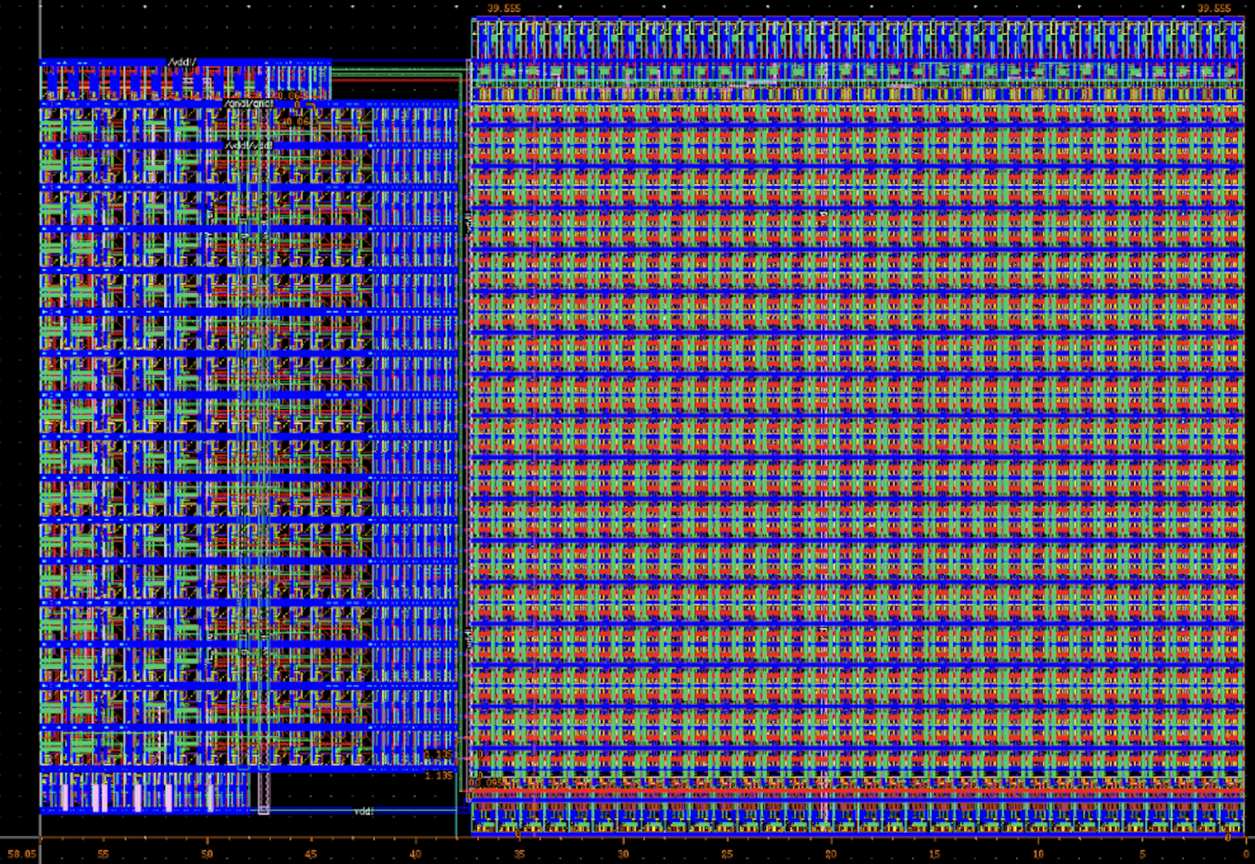
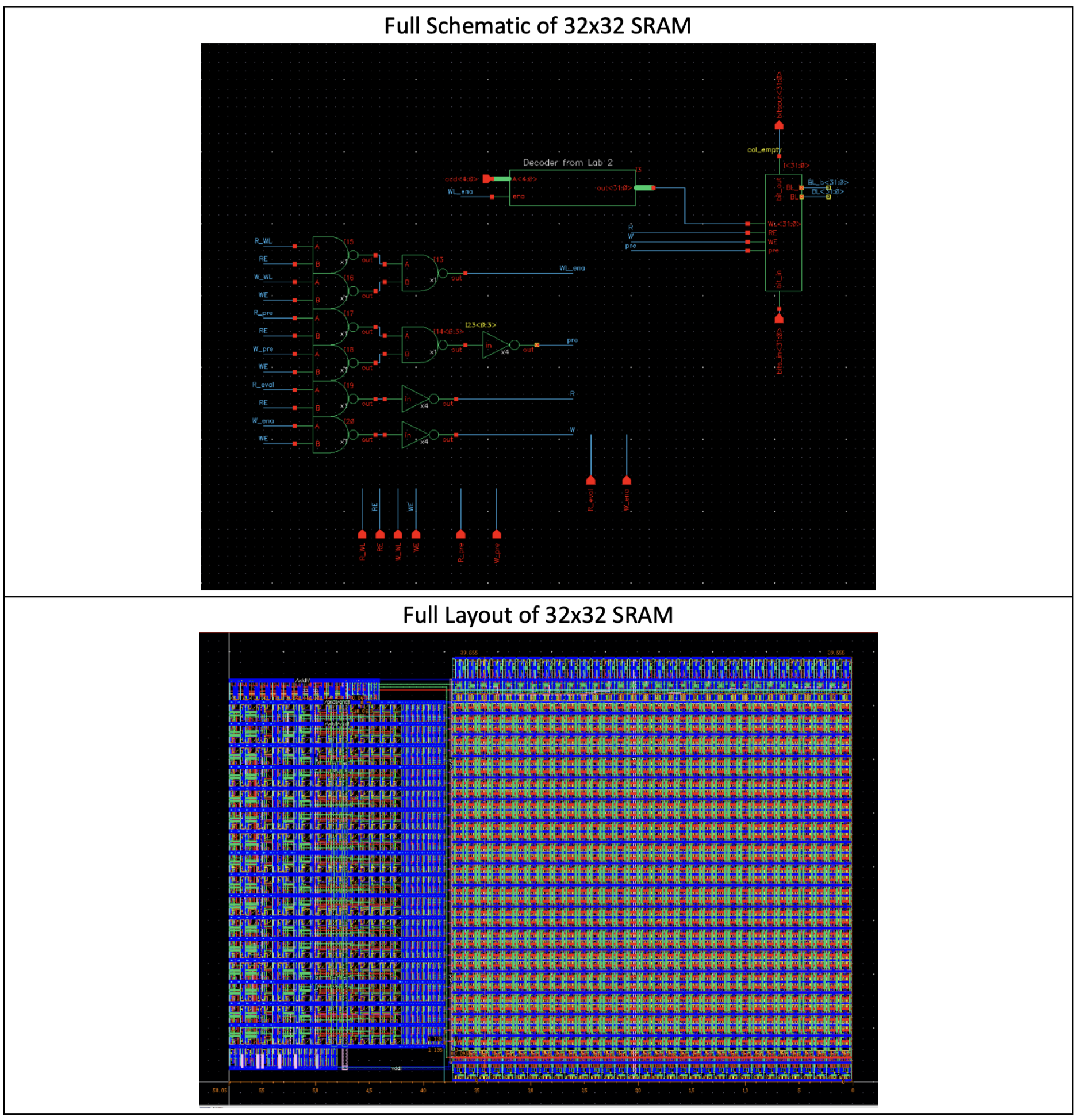
32×32
Array size
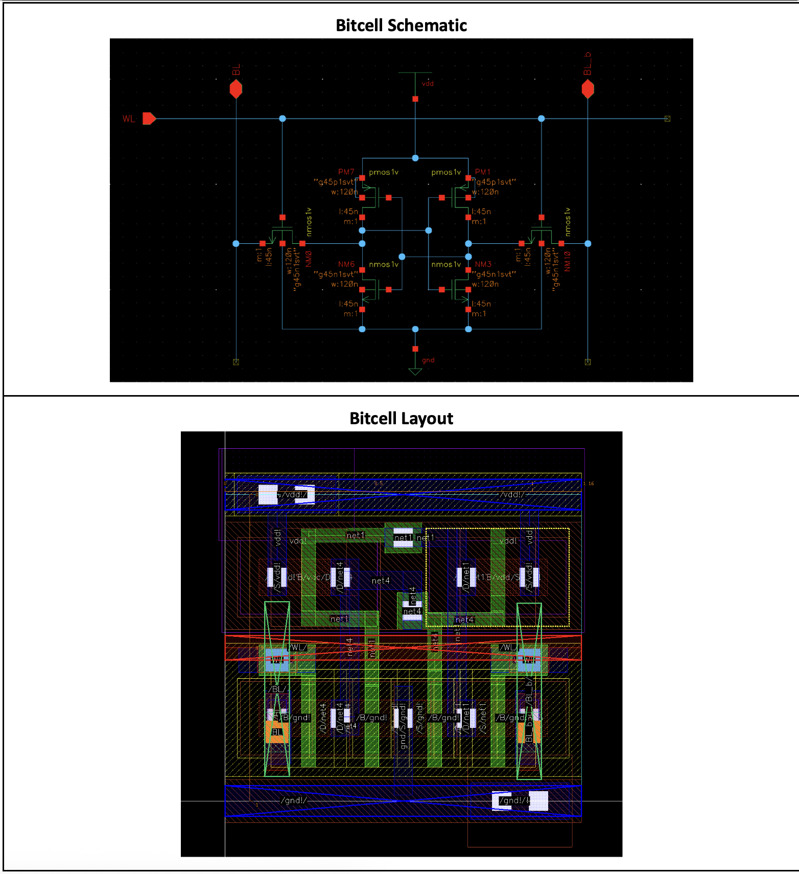
6T
Bitcell type
SRAM
VLSI
Cadence Virtuoso
6T Bitcell
Layout
DRC/LVS
Monte Carlo
Summary
As part of Cornell's Digital VLSI Design course (ECE 4740), I developed a 1 kilobyte (32×32) 6T SRAM array from schematic to layout using Cadence Virtuoso. Post-layout simulations confirmed a 600ps cycle time with a read energy of 14.2fJ/bit. The design passed DRC and LVS clean after resolving layout spacing violations.
Team Division of Work
The array was partitioned into sub-cells, each designed and verified by a separate team member before integration:
- Bitcell: 6T SRAM cell with optimized transistor sizing for read stability and write margin
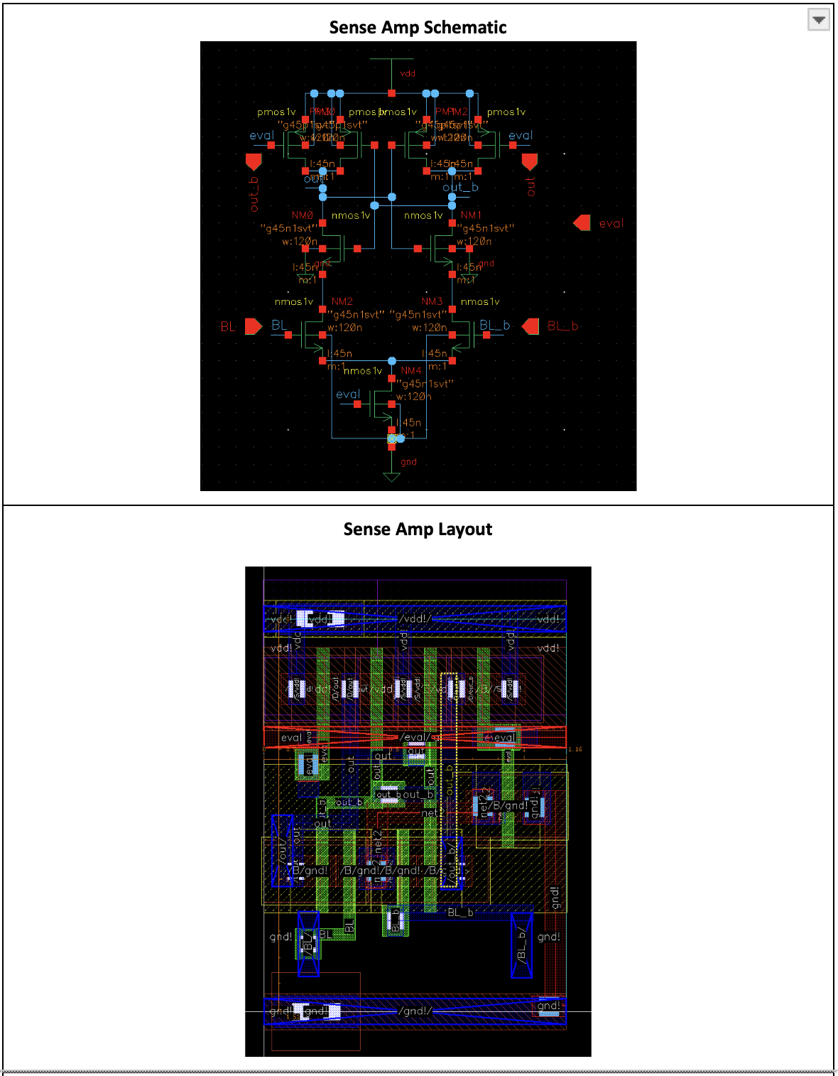
- Sense Amplifier: Differential sense amp for fast, low-power bit-line read
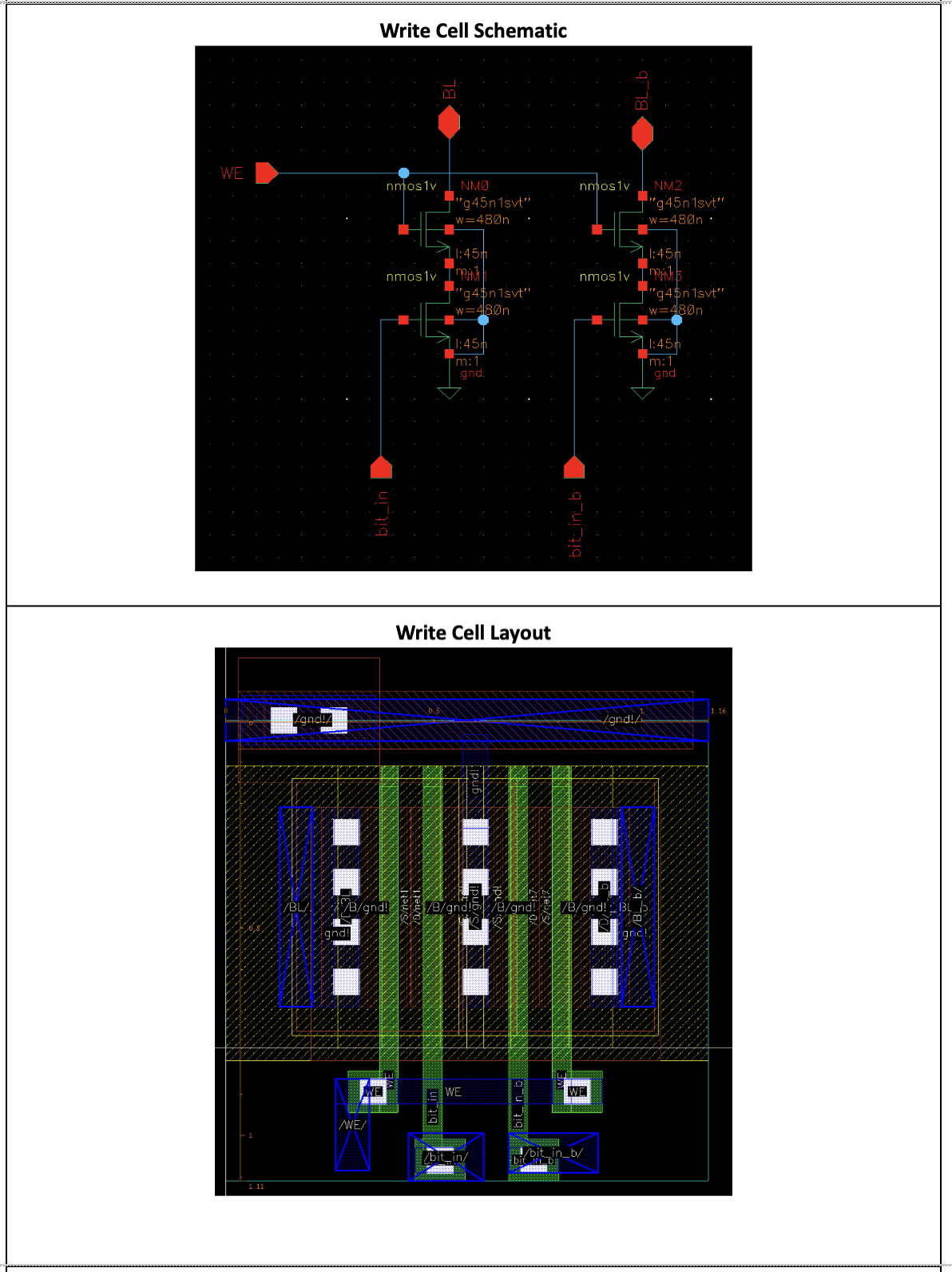
- Write Circuit: Write driver for forcing bit-line voltages during write operations
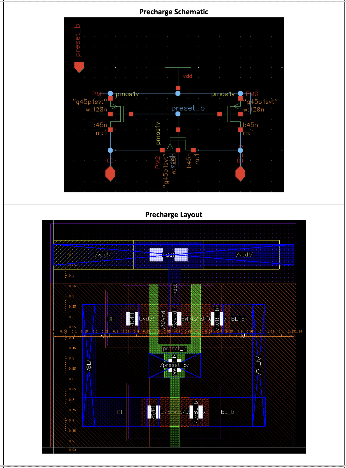
- Precharge (my contribution): Compact precharge circuit to equalize bit lines before each read cycle, optimized for minimal area impact on the array footprint
Verification
After sub-cell integration, the full array underwent:
- 32-bit column simulation to verify bit-line sensing across all columns simultaneously
- Monte Carlo simulation to characterize read/write margin across process, voltage, and temperature corners
- Full-array post-layout SPICE simulation confirming the 600ps cycle time and energy targets