Project information
- Course: ECE 5760 — FPGA & Hardware Accelerator Design
- Date: January 19 – February 2, 2026
- Platform: Intel Altera DE1-SoC
- Tools: Quartus Prime, ModelSim, Qsys (Platform Designer)
- Demo: YouTube
- Report: Lab Report
Summary
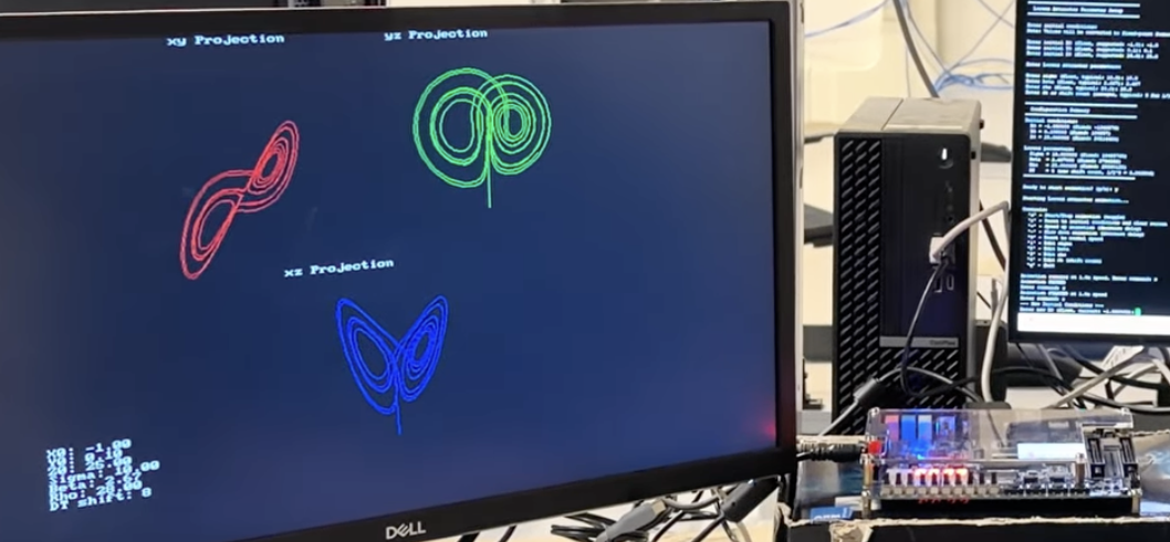
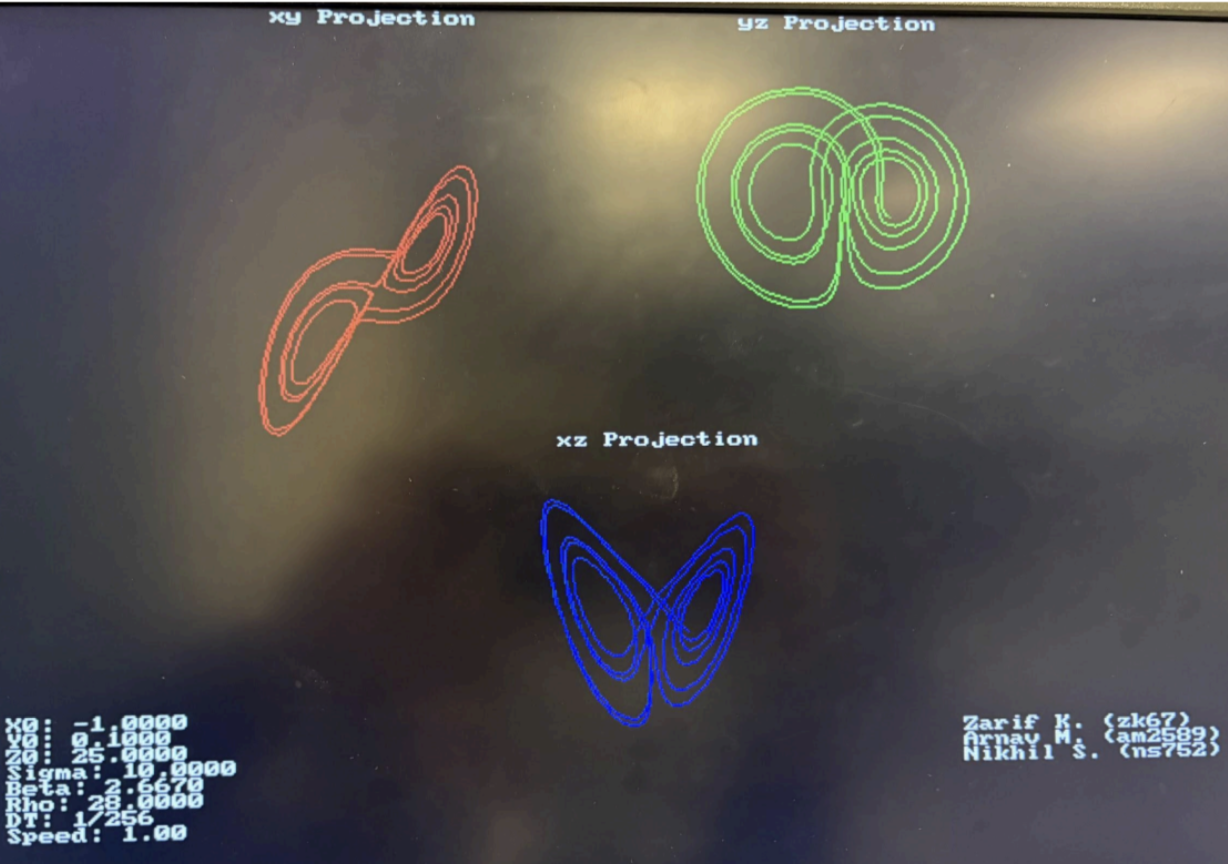
As part of Cornell's FPGA & Hardware Accelerator Design course (ECE 5760), my group implemented a hardware ordinary differential equation solver for the Lorenz system on an Intel Altera DE1-SoC FPGA. The system solves the three coupled differential equations in real time and streams the result to a VGA monitor, rendering the characteristic Lorenz attractor trajectory.
The Lorenz System
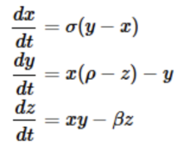
The Lorenz system is a set of three ODEs that exhibit chaotic behavior — small changes in initial conditions produce wildly divergent trajectories. Solving it requires continuous integration of:
- dx/dt = σ(y − x)
- dy/dt = x(ρ − z) − y
- dz/dt = xy − βz
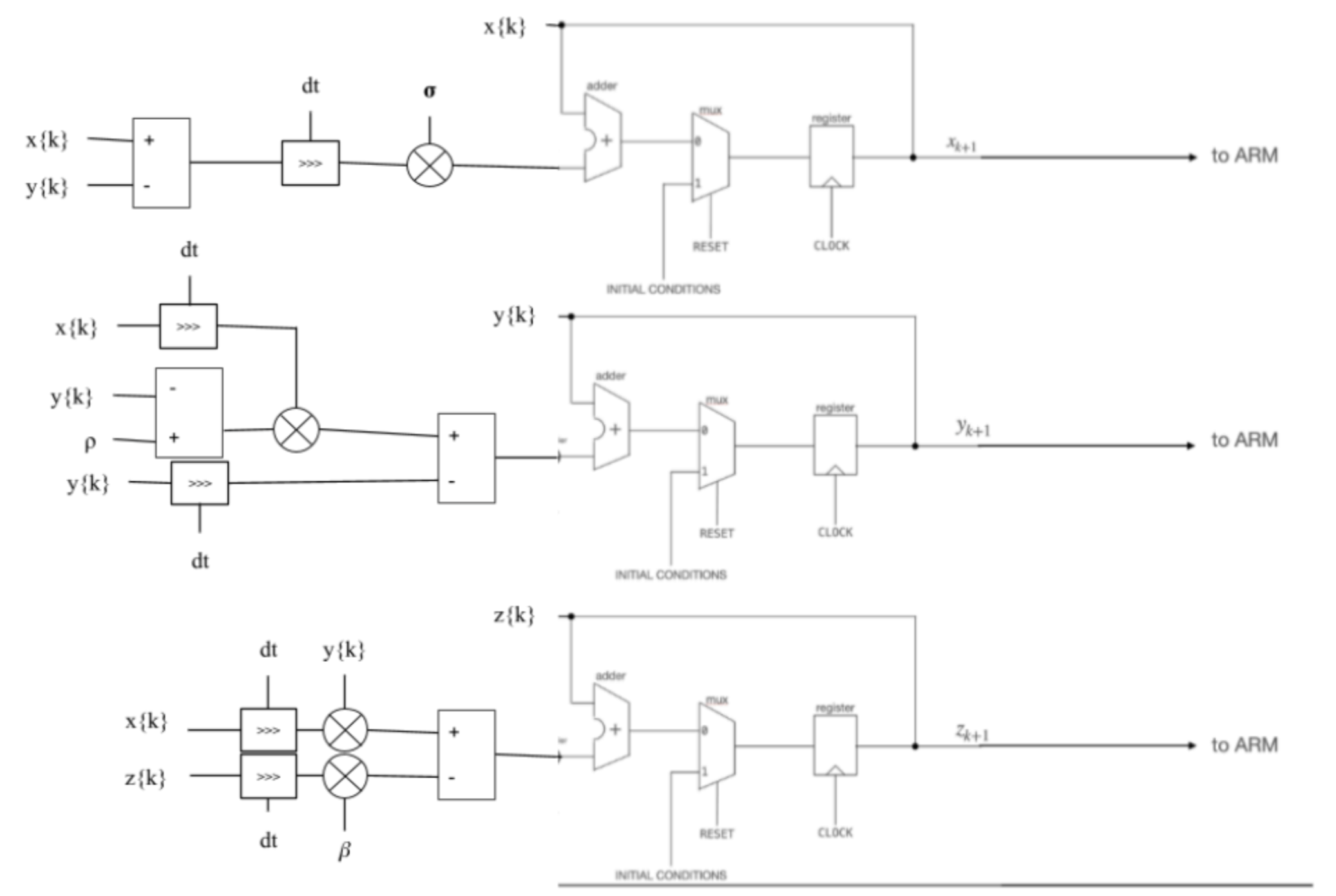
The hardware solver uses fixed-point arithmetic to iteratively update the state at each clock cycle, using forward Euler integration. The resulting x-y trajectory is rendered to the VGA framebuffer.
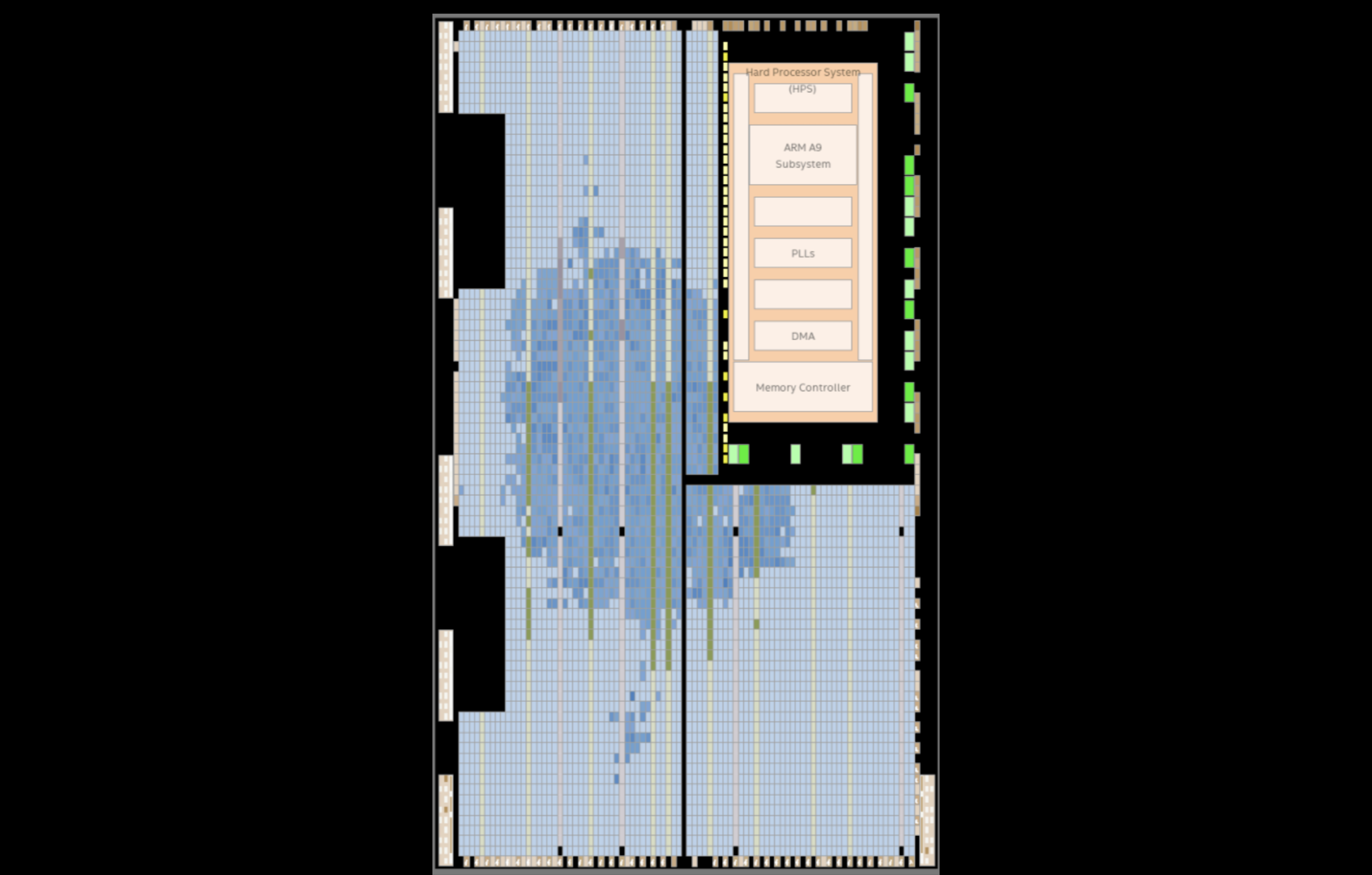
Hardware Architecture
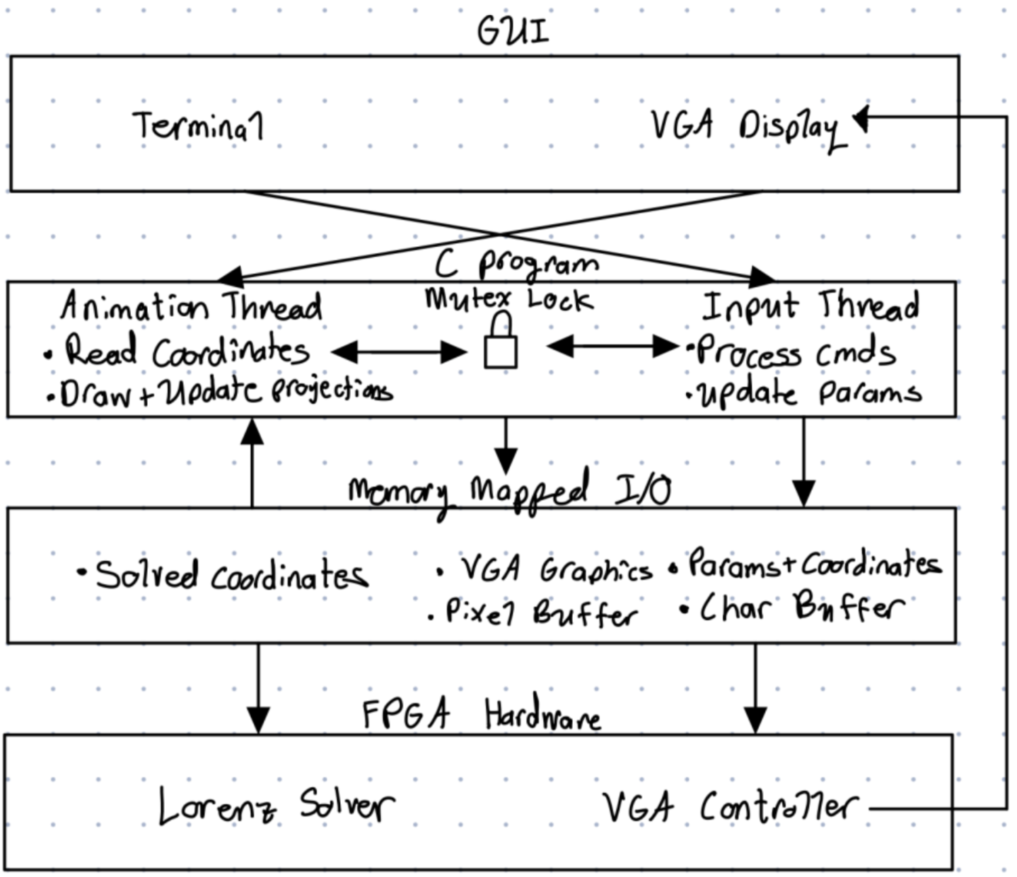
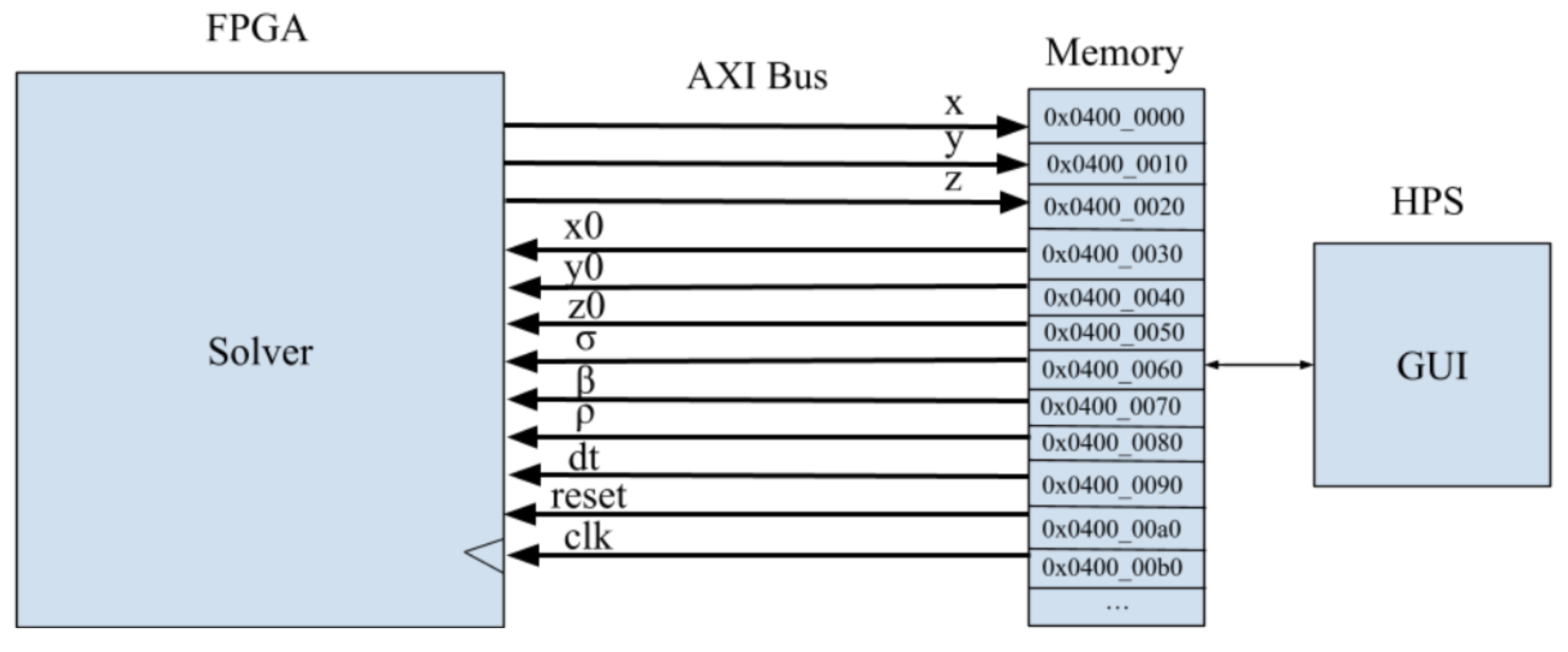
The system is structured as a memory-mapped hardware/software co-design on the DE1-SoC:
- The Verilog ODE core performs all multiplications and additions each cycle in fixed-point
- Platform Designer (Qsys) maps the core's state registers to the HPS address space
- The HPS (ARM A9) handles user input for σ, ρ, β parameters and initial conditions
- VGA output is driven directly from the hardware-computed x-y coordinates