Project information
- Course: ECE 5760 — Hardware Acceleration via FPGA
- Date: April 2026 – May 2026
- Team: Zarif Karim, Arnav Muthiayen, Nikhil Sampath
- Platform: Intel Altera DE1-SoC
- Tools: Verilog HDL, Quartus Prime, ModelSim, Platform Designer (Qsys), ARM A9 HPS Linux + C
- GitHub: aes128_de1soc_fpga
- Full Report: Cornell ECE 5760
- Demo: YouTube
Introduction
This project implements AES-128 encryption and decryption on the DE1-SoC FPGA, demonstrated by encrypting image data and displaying the result through a real-time VGA output. The project was motivated by the importance of accelerating security workloads so that cryptographic operations do not become a performance bottleneck in modern systems.
In the final design, the HPS (ARM A9) loads image data, packs pixels into 128-bit blocks, sends them to the Verilog AES engine on the FPGA fabric, and streams the processed output to the VGA display buffer. The completed system supports encryption and decryption of multiple images with user-selected 128-bit keys.
AES-128 Background
AES (Advanced Encryption Standard) is a symmetric key block cipher — the same key is used for both encryption and decryption. AES-128 operates on 128-bit data blocks with a 128-bit key over 10 rounds of transformation. Each round applies four operations:
- SubBytes — Non-linear SBox lookup substitution of each byte
- ShiftRows — Cyclic left rotation of each row to rearrange bytes across columns
- MixColumns — Column mixing to spread information across the block (skipped in the final round)
- AddRoundKey — XOR of the current state with the round key
Key expansion generates 11 round keys (1 initial + 1 per round) using byte rotations, SBox substitutions, and XOR with Rcon constants. Decryption applies the inverse operations in reverse order. The algorithm is bit-exact and fully lossless.
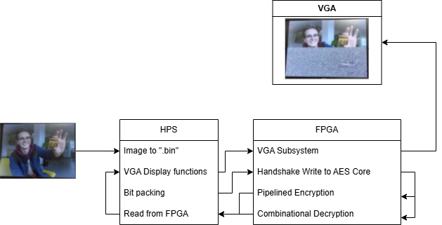
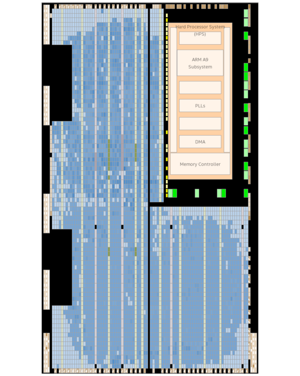
System Architecture
The system is a hardware-software co-design pipeline across HPS and FPGA:
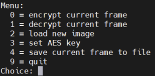
- HPS (software): Image loading (640×480 RGB565 .bin files), terminal menu, key entry, VGA display coordination, and block I/O to the FPGA via memory-mapped PIO
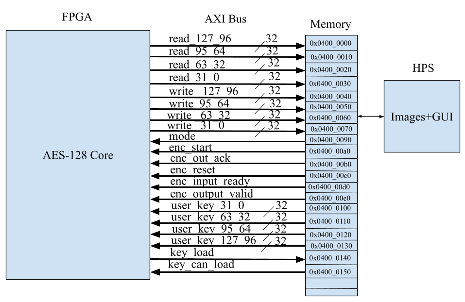
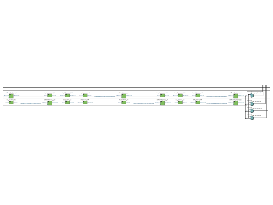
- FPGA (hardware): Pipelined 10-round AES-128 encryption datapath, combinational AES-128 decryption datapath, 11-round key expansion module, and an output FIFO decoupling the pipeline from HPS reads
Pixel data is packed into 128-bit blocks of 8 pixels (16-bit RGB565 each) and transferred via four 32-bit PIO writes. A ready/valid/ack handshaking protocol manages the pipeline flow. The PIO-based communication through the AXI heavyweight bus is the dominant bottleneck — not the AES core itself.
Hardware Design — Pipelined Encryption
The encryption datapath is fully pipelined: an initial AddRoundKey stage (round key 0), rounds 1–9 applying the full four-operation sequence, and a final round omitting MixColumns. Pipeline registers between each stage carry both the 128-bit state and a valid bit, enabling one new block to be accepted every clock cycle at steady state.
A small output FIFO decouples the encryption pipeline from HPS reads. It tracks write/read pointers and occupancy, asserting ready when space exists and valid when output is available. The HPS dequeues results by reading the output PIOs and pulsing an ack signal.
Hardware Design — Decryption
Decryption applies the inverse operations in reverse order through a combinational (non-pipelined) datapath: AddRoundKey with the final encryption round key, then per-round inverse ShiftRows → inverse SubBytes → AddRoundKey → inverse MixColumns (final round omits inverse MixColumns). The same expanded round keys generated for encryption are reused in reverse order.
Performance Results
Clock: 50 MHz FPGA PLL. Full 640×480 frame = 38,400 AES blocks. Default test key: 000102030405060708090a0b0c0d0e0f.
| Operation | Implementation | Time (ms) | Speedup |
|---|---|---|---|
| Encrypt 640×480 | ARM software | ~1179 | 1.0x |
| Encrypt 640×480 | Pipelined FPGA | ~264 | ~4.5x |
| Decrypt 640×480 | ARM software | ~8970 | 1.0x |
| Decrypt 640×480 | Combinational FPGA | ~2461 | ~3.6x |
Speedup is consistent across image content, confirming it is structural rather than data-dependent. The bottleneck is PIO bus bandwidth (~4 writes + 4 reads + handshake pulses per block), not the AES core. The pipelined core is theoretically capable of one block per cycle — well under 1 ms for a full frame.
Resource Utilization
| Resource | Usage |
|---|---|
| ALMs | 27,575 / 32,070 (86%) |
| ALUTs | 36,717 / 64,140 total |
| Dedicated Logic Registers | 11,537 |
| M10K Blocks | 16 / 396 (4%) |
| DSP Blocks | 6 / 87 (7%) |
| Compile Time | ~30 minutes |
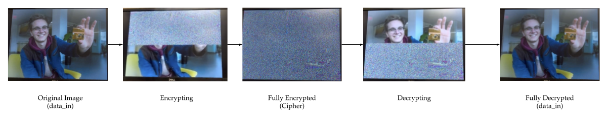
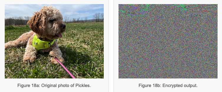
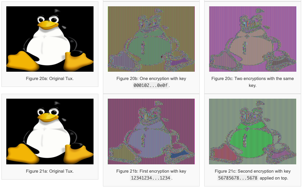
Visual Results & ECB Mode Weakness
Encrypted images appear as noise. The project demonstrates a well-known ECB (Electronic Codebook) mode weakness: when an input has large uniform-color regions (e.g., the Cornell logo, the Tux penguin), identical plaintext blocks encrypt to identical ciphertext blocks — leaving the underlying shape faintly visible in the encrypted output.
Correctness was verified two ways: (1) walking the hardware through the NIST FIPS 197 Appendix B worked example bit-for-bit, and (2) cross-checking pipelined FPGA output against a pure-software C AES implementation on the same image and key — the encrypted .bin files were identical at every pixel.
Conclusions & Future Work
The system achieved a 4.5x encryption and 3.6x decryption speedup over the software ARM baseline while staying within 86% ALM utilization and passing NIST FIPS 197 verification. The ECB-mode weakness demonstration provided a visually compelling cryptographic lesson.
Key takeaway: even after accelerating computation, the system is only as fast as its slowest link. The PIO bus, not the AES core, was the bottleneck throughout. Future improvements:
- Replace per-block PIO transfers with DMA-style burst transfers from SDRAM directly into the AES core
- Implement proper ready/valid/ack handshake for the decryption path
- Pipeline the decryption datapath to match encryption throughput
- Add CBC (Cipher Block Chaining) mode to eliminate ECB outline artifacts