Project information
- Course: ECE 6745 — Complex Digital ASIC Design
- Date: March 2026 – April 2026
- Team: Zarif Karim, Vaishnavi Vednere, Vinay Ivaturi
- Technology: TSMC 180nm
- Tapeout: 1mm × 1mm ASIC chip
- Tools: PyMTL3, Synopsys VCS, Synopsys PT, Cadence Innovus (PnR), Mentor Calibre (DRC/LVS)
- Presentation: Google Slides
Introduction
Genomics requires more memory and computation than nearly any other field of research. Rapid growth of genomic data creates a critical bottleneck: aligning DNA sequences against each other at scale is both memory- and compute-intensive. Building a dedicated hardware accelerator is a powerful workaround to the limited throughput and parallelism of general-purpose CPUs.
As part of Cornell's ECE 6745 Complex Digital ASIC Design course, our team of three designed and taped out a Smith-Waterman algorithm accelerator targeting the TSMC 180nm node. The chip fits within a 1mm × 1mm footprint alongside the course's shared processor baseline and was submitted for fabrication in summer 2026.
Smith-Waterman Background
Smith-Waterman is the gold standard algorithm for local sequence alignment: finding the most similar region between two DNA sequences, rather than forcing end-to-end alignment. It operates by building an (N+1) × (N+1) scoring matrix from two input sequences of length N. Each cell stores the best alignment score reachable at that position.
Three candidate scores are computed per cell:
- Diagonal — match/mismatch between the two current bases (+1 match, −1 mismatch)
- Left — a gap in sequence 2 (−2 penalty)
- Above — a gap in sequence 1 (−2 penalty)
The cell is assigned the maximum of the three candidates, floored at 0 (no negative scores). After filling the entire matrix, the maximum score across all cells is the local alignment score. Traceback to recover the optimal aligned sub-sequence is a separate step that was scoped out of this accelerator to meet area constraints.
Our accelerator takes two 16 base-pair DNA sequences (each base pair 2-bit encoded: A=00, C=01, G=10, T=11) and outputs the maximum alignment score.
Design Space — Four Axes of Exploration
The Smith-Waterman DP problem has a rich hardware design space. We explored four orthogonal axes:
Calculation Style
- Row-chunk (baseline)
- Anti-diagonal (final)
Pipelining
- Combinational PE's
- Sequential PE's
Data Streaming
- Bulk load
- Base forwarding
Dimensionality
- 16×16 array
- 8×8 tiled (final)
The software baseline computes the matrix row-by-row — a "sliding window" that evaluates each row sequentially, limited by data dependencies that prevent parallelism and by high cycle counts per row. The hardware breaks these dependencies by exploiting the anti-diagonal structure of the DP graph.
System Architecture — 8×8 Systolic Array
The final accelerator is an 8×8 systolic array of 64 processing elements (PEs), paired with an 8×8 score buffer. The key insight: within the scoring matrix, cells on the same anti-diagonal are fully independent of each other — each only depends on its diagonal-left, top, and left neighbors, which belong to the previous anti-diagonal. This allows all cells on the same anti-diagonal to be computed simultaneously.
Rather than building a full 16×16 array (256 PEs), the 8×8 array tiles across the larger 16×16 scoring matrix. The design maintains:
- Top row buffer — stores the bottom row of the previous tile row for use as the "above" input in the next tile row
- Left column buffer — stores the rightmost column of the previous tile column for "left" inputs
- Corner register — captures the single corner value at tile boundaries
At each cycle, only the PEs on the active anti-diagonal are computing; others idle. This strict scheduling ensures all required inputs are ready from the previous cycle. Data flows locally between neighbors, eliminating global communication — the defining property of a systolic architecture.
Each PE: receives diagonal, top, and left score inputs; compares the two incoming DNA bases; computes all three candidate scores; outputs the max (floored at 0); and forwards its base and score to adjacent PEs.
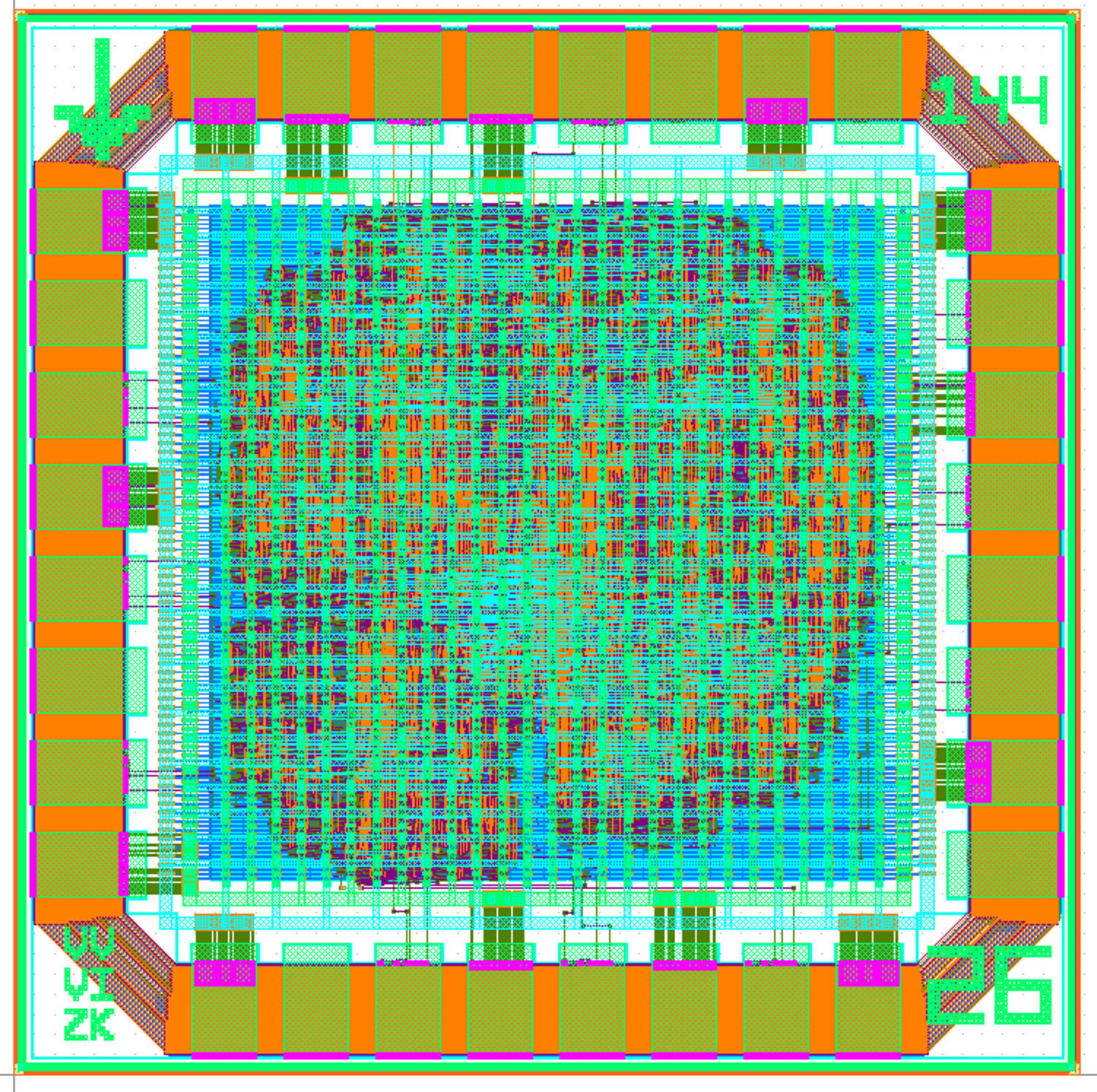
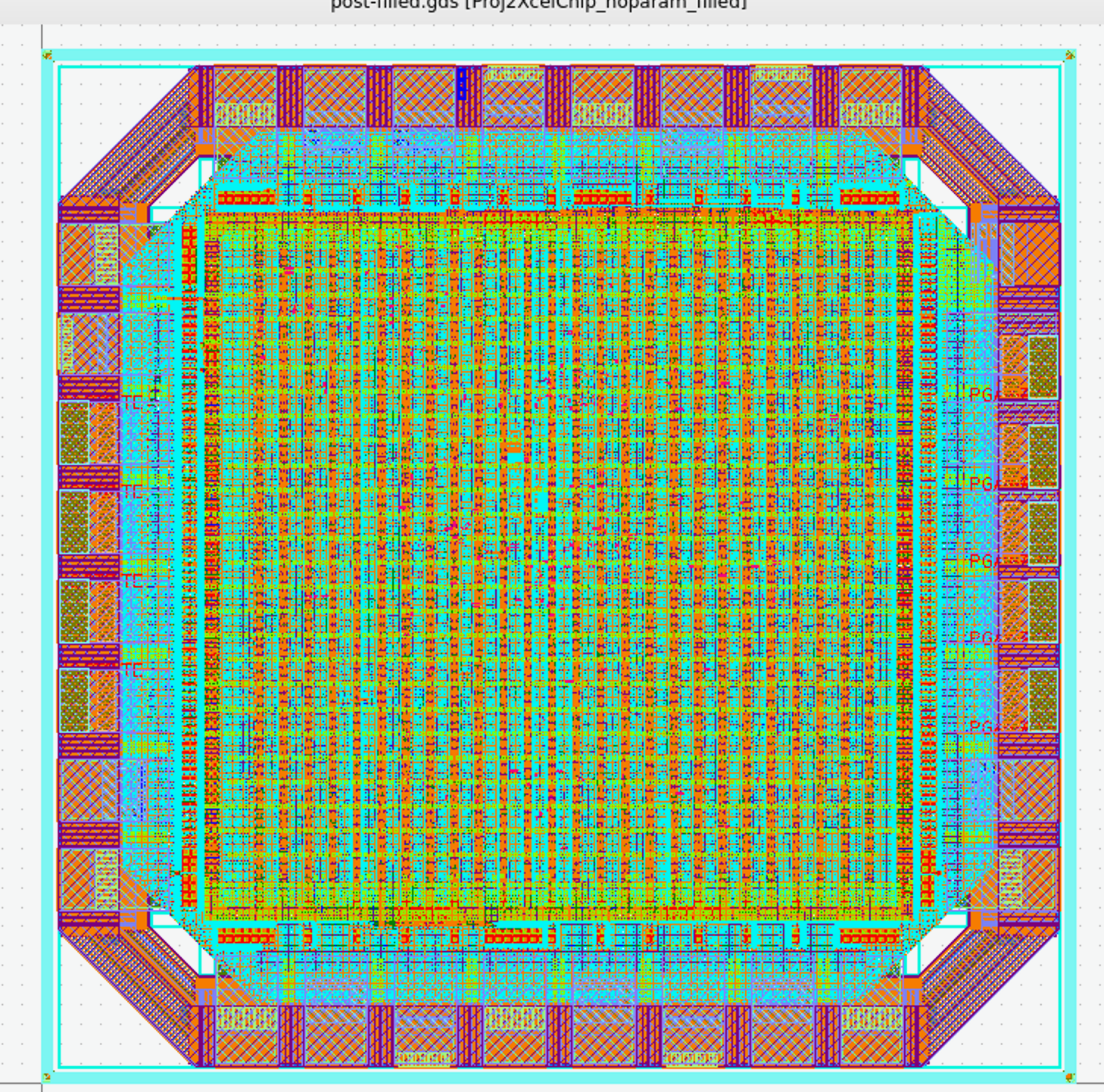
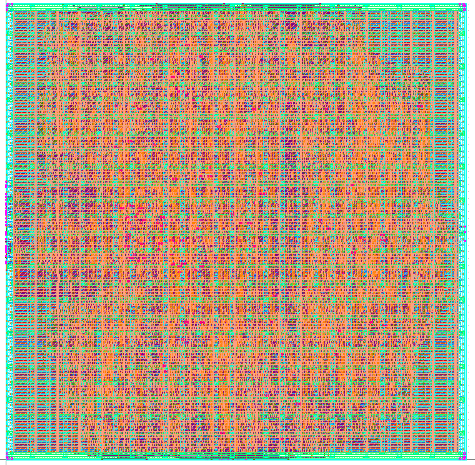
RTL → Synthesis → Place and Route → Tapeout Flow
The complete ASIC implementation flow used industry-standard EDA tools:
- RTL Simulation: PyMTL3 RTL sim + Synopsys VCS (71/71 test cases passed at both RTL and gate level)
- Synthesis: Synopsys Design Compiler — 7,904 standard cells, 128,142 μm² block area, 0.0145 ns setup slack
- Place and Route: Cadence Innovus — 9,334 cells post-PnR, 60.39% density, 0.0812 ns setup slack, 0.0201 ns hold slack, clock insertion source latency = 0 ns
- Static Timing Analysis: Synopsys PrimeTime — 0.1107 ns setup slack, 0.0164 ns hold slack (timing clean)
- Physical Verification: Mentor Calibre DRC + LVS — no violations found
- Bag Sim: 71/71 passed (post-PnR functional verification)
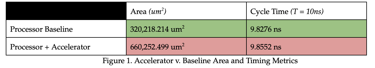
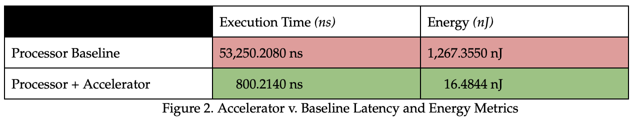
Performance Results
Clock period: 10 ns (100 MHz). Both the processor baseline and processor + accelerator meet timing.
| Metric | Processor Baseline | Processor + Accelerator |
|---|---|---|
| Area (μm²) | 320,218 | 563,936 |
| Cycle Time | 9.8276 ns | 9.8552 ns |
| Execution Time | 53,250 ns | 810 ns (66x faster) |
| Energy | 1,224.8 nJ | 13.8 nJ (76x less) |
The accelerator completes alignment in a fixed 77 cycles (770 ns) regardless of sequence content. Energy varies slightly across test cases due to differing match/mismatch rates but stays below 8.5 nJ per alignment. The massive energy reduction comes from eliminating repeated LOAD/ADD/BRANCH overhead — all computation flows directly through the PE array without memory round-trips.
Test Case Results
| Test Case | Cycles | Time (ns) | Power (mW) | Energy (nJ) |
|---|---|---|---|---|
| tc1-basic | 77 | 770 | 11.00 | 8.47 |
| tc2-all-mismatch | 77 | 770 | 9.36 | 7.20 |
| tc3-all-mismatch-alternating | 77 | 770 | 9.52 | 7.33 |
| tc4-partial-match-front | 77 | 770 | 9.95 | 7.66 |
| tc5-partial-match-mid | 77 | 770 | 10.10 | 7.78 |
| tc6-single-match | 77 | 770 | 9.40 | 7.24 |
| tc8-gap-shift-one | 77 | 770 | 11.00 | 8.47 |
| tc10-first-base-mismatch | 77 | 770 | 10.90 | 8.39 |
| tc11-gap-extra-base | 77 | 770 | 11.00 | 8.47 |
| tc12-two-gaps | 77 | 770 | 11.00 | 8.47 |
Resource Utilization
| Metric | Value |
|---|---|
| Block area constraint | 360,000 μm² |
| Synthesized area | 128,142 μm² (36% of budget) |
| Post-PnR cell area | 148,792 μm² |
| Post-PnR core area | 256,562 μm² (71% of budget) |
| PnR density | 60.39% |
| Standard cells (synthesis) | 7,904 |
| Standard cells (post-PnR) | 9,334 |
| DRC violations | None |
| Antenna DRC violations | None |
| LVS result | Clean (no violations) |
Design Observations & Tradeoffs
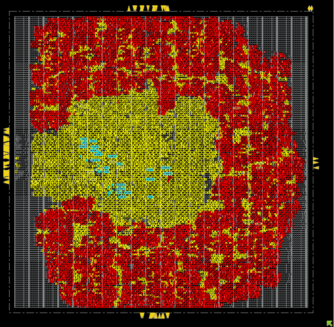
The main architectural tradeoff encountered was between control logic area and array size. With the 8×8 tiled approach, the control logic (tile state machine, boundary buffers, anti-diagonal scheduling) grew to rival the area footprint of the PE array itself — visible in the PnR layout where yellow control logic and red PE regions share roughly equal space.
A 16×16 array would eliminate tiling complexity (and the boundary buffer overhead) at the cost of 4× more PEs. A smaller tile (e.g., 4×4) would reduce control complexity but require more tiles and more boundary-crossing overhead per alignment.
Energy reduction is structural: a CPU executing Smith-Waterman must issue LOAD, ADD, CMP, and BRANCH instructions for every cell — each involving memory access and pipeline overhead. The systolic array feeds inputs directly into PEs each cycle, eliminating all that overhead. Less unnecessary work per operation = proportionally less energy.
Conclusions & Future Work
The tapeout-ready Smith-Waterman accelerator achieves a 66x execution time reduction and 76x energy reduction over the software baseline, completes in a fixed 77 cycles regardless of input, uses 71% of its area budget, and passes all DRC/LVS checks with no violations. The chip was submitted for fabrication in the TSMC 180nm node.
Key takeaway: hardware specialization for a specific algorithm — even implemented in an older process node — delivers order-of-magnitude efficiency gains that a general-purpose processor cannot match. The bottleneck shifted from computation to control logic overhead.
Future directions:
- Optimize tile controller to shrink the control logic area footprint
- Extend to variable-length sequences (current design is fixed at 16 bp)
- Add traceback logic to recover the optimal aligned sub-sequence, not just the score
- Explore a 16×16 array to eliminate tiling overhead and reduce control complexity
- Port to a more advanced node (e.g., TSMC 65nm or 28nm) to further improve PPA